Solutions for Custom IC design

Custom IC Design
Complete integrated design tool flows for analog, RF and mixed signal IC design down to 12nm.

IC Test
Tessent Design-For-Test help ensure the highest test coverage, accelerate yield ramp and improve the quality and reliability of manufactured parts.

Analog /Mixed-Signal Verification
A comprehensive verification portfolio for custom analog and mixed-signal IC design

Integrated Photonics
A photonics solution for the IC designer integrating photonics into the IC.

Physical Verification
Physical verification for IC design with Siemens EDA industry leading solution, Calibre®, for accuracy, reliability, and performance.

MEMS Design
A MEMS foundry-proven design flow with 3D design and fabrication. Built on the gold standard for MEMS layout implementation and enables integration of the MEMS device with IC circuitry.
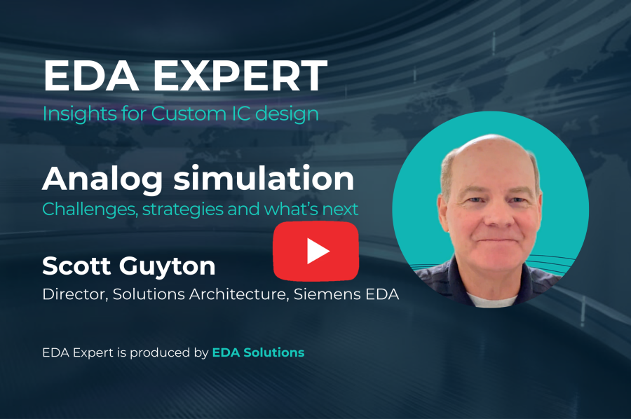
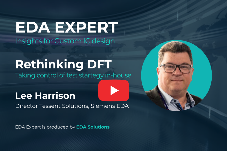
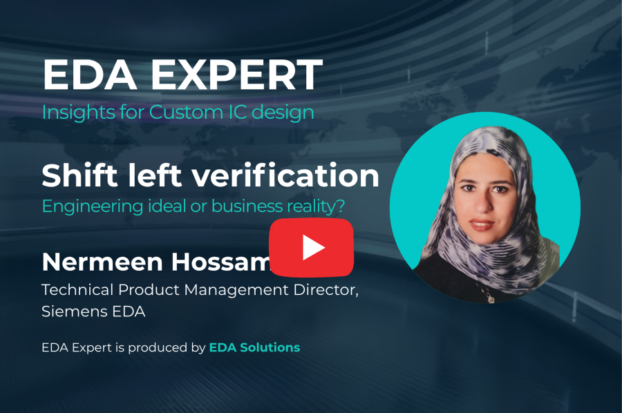
EDA Expert : Insights for Custom IC design
The EDA Expert interview style series is designed to help start-ups and small-to-medium enterprises navigate the increasingly complex landscape of electronic design automation tools and solutions.
Each episode will feature an in-depth conversation between EDA Solutions host and an EDA Expert, focusing on a specific design challenge or solution.
Services to enhance your business

EDA Solutions strives to provide the best possible advice and training, enabling customer to maximise the return on their investment in Siemens EDA.
In this spirit, we have implemented a Custom Success Management (CSM) program and introduced three new service-based products.
The CSM program will make us more proactive supporting customers like yourself. And the new service products employ our specialist EDA know-how and experience to work for you, freeing your resources to focus where it matters most, chip design.
- Managed EDA – Outsource EDA tool and PDK set-up to EDA experts.
- Managed Cloud – Take advantage of AWS cloud compute power to scale with your requirements.
- Premium Support – Engage for higher priority projects or to always prioritise your engineer’s productivity.
Video resources

On-demand webinars
Missed the live session? No problem. Access our webinars and watch at your convenience.

Quick Videos
Discover your “Aha!” moment. A series of ‘self-service’ videos designed to introduce a new topic, tool or feature in about 2 mins.
Products
Custom IC’s require specialist design tools to go from concept through to GDSII tape out. Learn about the IC design flow we offer.

Business & help
Discover EDA Solutions’ values and guiding principles, as well as the tools we provide to support customers can help you.
What customers say…

Upcoming events and latest news
-
Secure and scalable AWS® architecture for the Siemens EDA Custom IC Design Flow
Secure and scalable AWS® architecture for the Siemens EDA Custom IC design flow Summary EDA Solutions provides a secure and scalable Amazon Web Services platform…
-
EDA Solutions at Image Sensors Europe 2026
EDA Solutions is delighted to share that we will once again exhibit at Image Sensors Europe, the premier technical and business event for the global…
-
EDA Solutions launches “EDA Expert” video series to demystify design challenges for European IC designers
Regular, on-demand program delivers breakthrough insights on AI-enabled and traditional solutions — without the hype — to help resource-constrained start-ups…