EDA Solutions logo

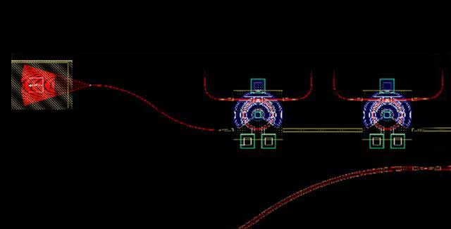
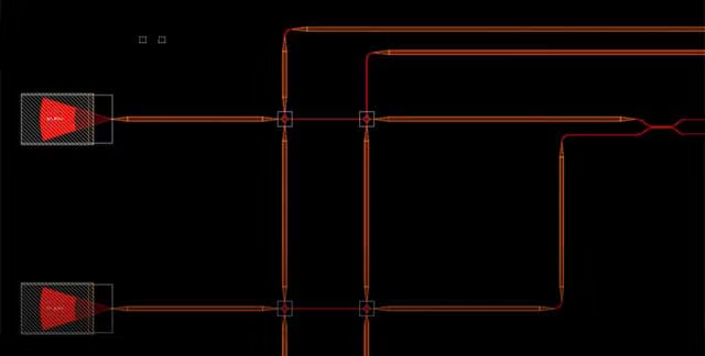
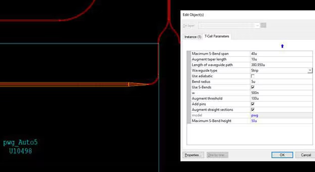
Design your photonic integrated circuit in a layout centric flow.  

The designer can implement their design using either a drag and drop or a script-driven methodology.  

Design in the same full custom IC design layout editor that drives the physical verification and tape-out processes.


Layout centric design

  • PIC design in a complete IC layout editor,
  • Create layout without writing a line of code
  • Supports a layout centric design flow where a schematic is not needed
  • Schematic flow optional with S-Edit
  • A simulation netlist can be created as input into a photonic simulator

Simplifying Photonic layout

  • Simple waveguide creation and editing
  • Automated crossing insertion
  • Precision snapping to optical pins
  • Wave guide to pin checking

Complete PIC design flow

  • Photonic layout verification with Calibre’s equation based design rules
  • Simulation is supported though integration with partners
    • Ansys, Luceda, Optiwave, and VPIphotonic
  • Photonic PDKs are available from multiple foundries
  • Scriptable with Python
  • Available on both Linux® and Windows®