Secure and scalable AWS® architecture for the Siemens EDA Custom IC design flow
Summary
EDA Solutions provides a secure and scalable Amazon Web Services platform purpose-built for Siemens EDA Custom IC Design (Tanner) environments. The solution enables semiconductor companies to access high-performance EDA infrastructure without managing complex IT, EDA or licensing operations internally. The architecture combines secure VPN access, NICE DCV remote visualisation, dynamically scalable simulation compute, encrypted storage, automated backups and centralised SALT (Siemens Advanced Licensing Technology). Supporting Siemens EDA tools including S-Edit software, L-Edit software, Solido™ software and Calibre® platform, the platform delivers enterprise-grade cloud infrastructure and operational expertise tailored for analogue, digital and mixed-signal IC development.
Introduction
The Siemens EDA Custom IC Design Flow is widely used for the development of analogue, mixed-signal and digital integrated circuits. The workflow typically involves multiple stages including schematic design, RTL development, layout creation, verification and circuit simulation.
These stages require specialised EDA tools and substantial computing resources. Simulation workloads in particular can be compute intensive, often requiring large numbers of CPUs to complete verification tasks in a reasonable time frame.
In analogue and mixed-signal (AMS) development, simulation demand grows significantly when validating complex circuits such as image sensors, data converters, PLLs, power management ICs, RF front ends and large memory arrays used in AI compute. These designs require extensive Monte Carlo analysis, corner verification and post-layout parasitic validation to ensure silicon robustness and manufacturing yield.
Traditional on-premises infrastructure presents several challenges:
- Simulation queues that stall tapeouts
- CapEx that burns runway before a single wafer is spun
- Hardware sitting idle while engineers wait for the next crunch
Cloud computing solves all three: on-demand capacity, zero idle CapEx and elastic scale exactly when verification demands it.
Siemens EDA Custom IC Design flow
From schematic to GDSII in a single, cloud-hosted flow
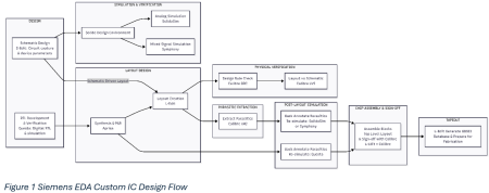
The flow moves through five distinct stages, each building on the last.
Design capture starts in S-Edit for analogue and Questa™ platform Questa™ software for digital RTL — schematic and logic defined, simulated and confirmed before a single piece of layout begins.
Simulation and verification are orchestrated through the Solido™ Design Environment software. Solido™ Sim software handles analogue, Symphony™ platform tackles mixed-signal. For AMS designs — image sensors, analogue front ends, high-speed interfaces which this means large-scale Monte Carlo, corner and variation-aware runs that expose problems before they reach silicon.
Layout translates verified designs into physical geometry. Analogue blocks are placed and routed in L-Edit; digital logic is synthesised and implemented in Aprisa™ software Aprisa™ solution, then integrated into the top-level layout alongside the analogue work.
Physical verification with Calibre confirms the layout is manufacturable. DRC checks every spacing and layer rule. LVS confirms the layout matches the schematic exactly. No connectivity errors, no fabrication surprises.
Parasitic extraction and post-layout simulation close the loop. Calibre xRC extracts the resistances and capacitances introduced by real interconnects. Those parasitics are back-annotated and the design is re-simulated in SolidoSim, Symphony or Questa to confirm performance holds up in the real world. For precision analogue, CMOS image sensors and SRAM arrays, this step is non-negotiable.
With all blocks signed off, the design is assembled at top level, given final Calibre signoff, and exported as GDSII for the foundry. Tapeout done.
The AWS advantage
AWS is the right platform for IC design. It is scalable, flexible and built with an ecosystem of services that map directly to engineering workloads
Semiconductor design flows require significant computational capacity during simulation while maintaining secure access to sensitive intellectual property. AWS allows resources to scale dynamically so compute capacity can increase during simulation workloads and reduce when demand decreases. This elastic model removes the limitations of fixed on-premises infrastructure while maintaining a secure environment.
AWS provides several Amazon Elastic Compute Cloud (Amazon EC2) instance families designed for different workload types used within the design flow.
| EC2 family | Purpose | Typical usage in EDA flow |
| C-Series | Compute optimised | Parallel circuit simulations and verification jobs |
| R-Series | Memory optimised | Interactive editor nodes running design tools |
| M-Series | Balanced general purpose | Infrastructure nodes such as jump hosts |
| T-Series | Cost efficient burstable | Lightweight services such as license servers |
The environment is deployed using AWS CloudFormation, allowing infrastructure to be created and reproduced automatically. Compute resources are delivered through EC2, while Amazon CloudWatch provides monitoring, logging and operational visibility across the system. Together these services enable a scalable, automated cloud platform capable of supporting demanding semiconductor design workloads.
Together, these instance families map precisely to the Siemens EDA workflow with no over-provisioning, no compromise.
Cloud architecture for Siemens EDA Custom IC Design flow
Figure 2 illustrates the secure AWS architecture used to deploy the Siemens EDA Custom IC design environment. Engineers access the system through a secure VPN connection and interact with the design tools using NICE DCV. The environment separates interactive design workloads from simulation compute resources while maintaining centralised licensing, encrypted storage and autoscaling compute capacity.
Architecture overview
The cloud environment is deployed within a secure Amazon Virtual Private Cloud (Amazon VPC). All compute resources are located inside a private subnet, ensuring that design infrastructure is not directly exposed to the public internet.
User access is controlled through a secure AWS VPN connection. Engineers must authenticate through the VPN before accessing any design resources within the cloud environment.
Once connected, engineers access the design environment using NICE DCV. NICE DCV provides high-performance remote desktop capabilities optimised for engineering and graphical workloads, allowing designers to interact with EDA tools with minimal latency.
The system architecture includes several key components:
- Head (aka Jump) node
- Editor node
- Compute nodes
- SALT license server
- Shared storage
- Load balancing and autoscaling infrastructure
Secure user access
Every part of the design environment sits inside a private subnet, unreachable from the public internet. Access requires VPN authentication without exception.
Once connected, engineers work through NICE DCV, which delivers encrypted remote visualisation sessions with the look and feel of a local desktop. Design tools respond as if they’re running on the engineer’s own machine.
IAM policies enforce least-privilege access throughout, ensuring every user and service has access only and exactly to what they need.
The result: a minimal attack surface, protected IP and an access model robust enough for the most sensitive design data.
Interactive design environment
The interactive design environment is hosted on a memory-optimised editor node.
This node contains the primary design tools used in the Siemens EDA Custom IC flow, including:
- S-Edit for schematic capture
- Questa for RTL development
- L-Edit for physical layout design
- Solido Design Environment (SDE) for test management
- Calibre for design verification
Engineers interact with these tools through NICE DCV sessions after connecting through the VPN.
To optimise costs, the editor node does not run continuously. When a user connects through the jump node, the system automatically activates the editor node. This ensures that compute resources are only consumed when actively required.
This on-demand activation model gives engineers a fast and responsive environment.
Simulation compute infrastructure
Simulation is where compute demands peak and the architecture dedicates a fleet of compute-optimised EC2 instances exclusively to the job.
AMS verification workloads require thousands of simulation runs across voltage, temperature, process and statistical variation conditions. Monte Carlo analysis for mismatch-sensitive analogue circuits and large memory structures creates substantial compute demand that scales beyond traditional workstation resources.
The compute nodes host Solido Sim, which executes simulation tasks generated from the design environment.
These compute nodes are associated with an autoscaling group, allowing the system to dynamically adjust the number of active compute instances according to workload demand. When simulation jobs increase, additional compute nodes are automatically launched. When demand decreases, unused instances are terminated to minimise cost.
A load balancer ensures that simulation jobs are distributed efficiently across the available compute nodes.
License management
Licensing for Siemens EDA tools is managed through a dedicated SALT license server hosted on a lightweight EC2 instance.
The license server provides licenses to both the editor node and compute nodes. Centralising license management ensures efficient utilisation of available licenses while maintaining consistent access control across the environment.
Because the license server requires minimal compute resources, it operates on a small instance to minimise infrastructure costs.
Storage and data protection
Design data is stored using encrypted Amazon Elastic Black Store (EBS) and Amazon Elastic File System (EFS).
All storage volumes are encrypted at rest to ensure protection of sensitive design information. Access to storage resources is restricted to authorised instances within the private network.
Backup policies are implemented according to customer requirements using AWS Backup. This ensures that design data can be recovered in the event of system failure or accidental deletion.
Shared storage enables design files, simulation results and verification data to be accessed by both editor and compute nodes.
Monitoring and operational visibility
Operational monitoring of the environment is handled through Amazon CloudWatch.
CloudWatch provides visibility into system performance, resource utilisation and system health. Metrics and logs collected by CloudWatch enable administrators to monitor infrastructure activity and identify potential issues.
The result is fully operational visibility together with the data to optimise cost and performance over time.
Cost optimisation strategy
Every design decision in this architecture targets cost efficiency:
- Editor nodes activate only when required
- Compute nodes scale dynamically based on workload
- Small instances are used for infrastructure services such as licensing
- Unused resources are automatically terminated
The result is enterprise-grade compute power without the cost of maintaining large on-premises clusters — pay for what you use, when you use it.
For AMS projects, where compute demand swings dramatically across the design cycle, this matters. Early-stage exploration needs modest resources; late-stage verification can demand massive simulation farms for corner analysis, yield validation and signoff. The architecture handles both without waste.
EDA Solutions: Your Siemens EDA cloud partner
Chip design is hard enough. Infrastructure shouldn’t slow you down.
EDA Solutions provides managed cloud expertise built specifically for Siemens EDA environments — so your engineers spend their time designing silicon, not wrestling with platform administration.
What we do
We architect, deploy and manage your entire cloud EDA environment:
- AWS infrastructure designed around Siemens EDA workflows
- Secure VPN and NICE DCV configuration
- License server integration and management
- Elastic compute scaling for simulation workloads
- Storage, encryption and backup strategy
- End-to-end workflow validation for analogue, mixed-signal and digital flows
Enterprise power. Lean team.
Start-ups and SMBs shouldn’t have to choose between world-class EDA capability and keeping the lights on. The compute capability of a major semiconductor house, without the overhead of running one.
From first commit to tapeout
Verification crunches, Monte Carlo runs, parasitic extraction — the demands on compute infrastructure peak exactly when you can least afford delays. EDA Solutions ensures your infrastructure is ready when it matters most, scaling rapidly and reliably through the most demanding phases of the design cycle.
The result: reduced deployment risk, predictable workflows, and teams that hit tapeout on schedule.
Conclusion
Designing custom ICs demands serious compute, secure infrastructure and tools that just work. The AWS architecture outlined here delivers all three — combining secure VPN access, NICE DCV visualisation, memory-optimised design environments and dynamic autoscaling into a platform built specifically for Siemens EDA workflows.
The result: faster verification cycles, lower operational overhead, and tapeout-ready teams that aren’t waiting on infrastructure.
EDA Solutions removes the complexity of cloud adoption so semiconductor design engineers can focus on what matters — designing and shipping silicon. Contact EDA Solutions today to accelerate your move to scalable, cloud-based IC design.